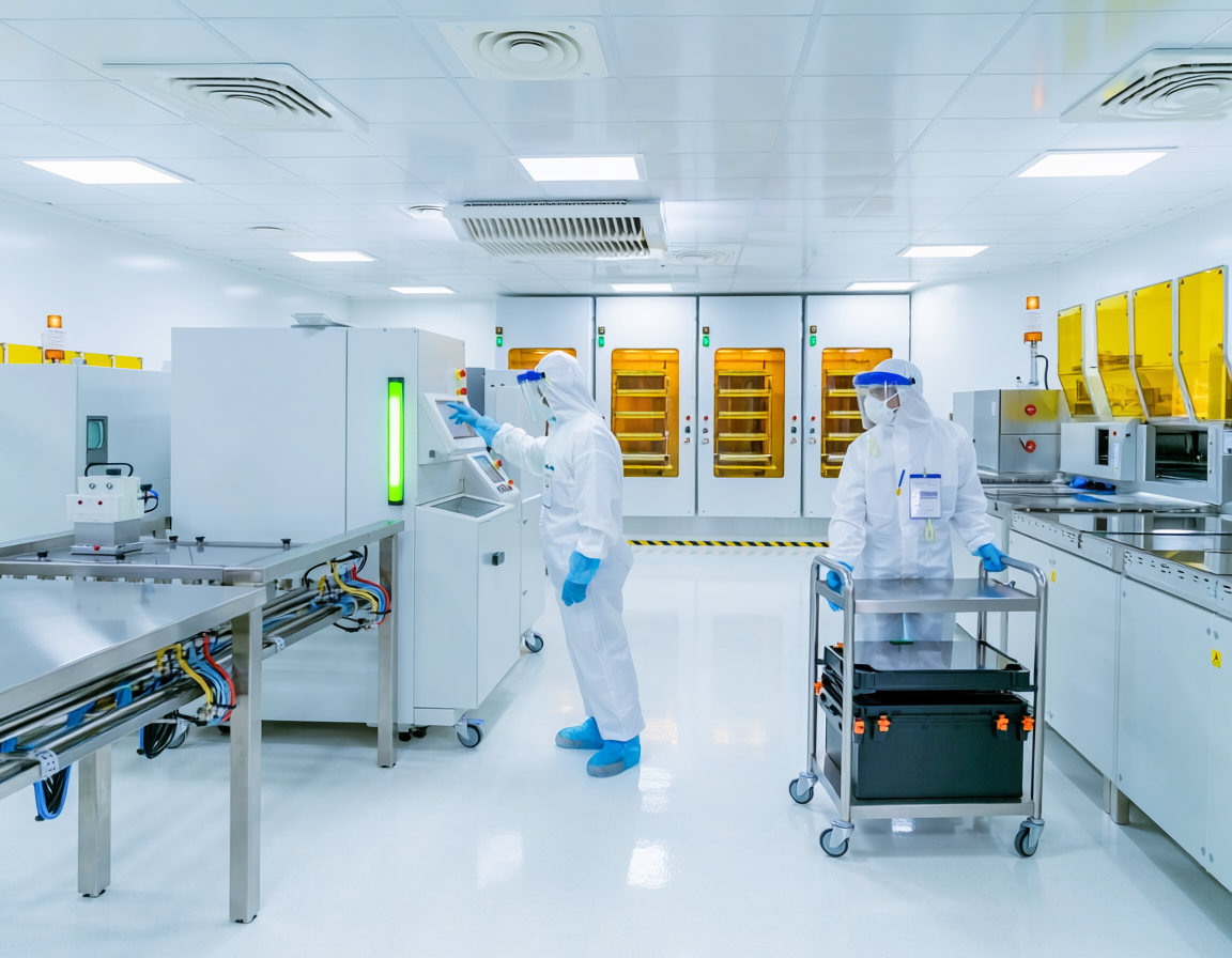
The message to suppliers was characteristically Musk: move at “light speed.” In the past few weeks, staff working on Terafab — the audacious semiconductor joint venture between Tesla, SpaceX, and xAI — have contacted chip equipment makers including Applied Materials, Tokyo Electron, and Lam Research, asking for price quotes and delivery timelines on a sweeping array of chipmaking gear. Photomasks, substrates, etchers, depositors, cleaning devices, testers — the full production stack. One supplier, according to people familiar with the matter, was asked on a holiday Friday to return a cost estimate by the following Monday.
The outreach, reported by Bloomberg, represents the first concrete operational steps toward Terafab since Musk officially unveiled the project on March 21, standing inside the defunct Seaholm Power Plant in downtown Austin with Texas Governor Greg Abbott in the audience. What was initially a spectacular announcement is now beginning its translation into phone calls, spreadsheets, and supplier negotiations. The gap between those two phases is where most of Musk’s grand visions either crystallise into reality or dissolve into expensive footnotes.
What Terafab Is Supposed to Be
Terafab, as Musk has described it, is not simply a chip factory. It is a vertical integration of the entire semiconductor manufacturing lifecycle under one roof — chip design, photolithography, fabrication, high-bandwidth memory production, advanced packaging, and testing — all co-located on the North Campus of Giga Texas in eastern Austin. The stated goal is one terawatt of annual computing capacity: more than all current global chip manufacturers combined can produce today, or even by 2030 based on projected industry growth.
The scale is deliberately staggering. Musk’s stated justification is equally blunt: “We either build the Terafab, or we don’t have the chips, and we need the chips, so we build the Terafab.” His case is that current suppliers — including TSMC, Samsung, and Micron — are expanding at a pace “much less than we would like,” and that the aggregate demand from Tesla’s Full Self-Driving software, its Optimus humanoid robot programme, SpaceX’s orbital data centres, and xAI’s AI infrastructure collectively requires between 100 and 200 billion custom AI chips per year. He has claimed that all the fabrication facilities on Earth currently produce only about 2% of what he will need.
The facility will produce two categories of chips. The first is an edge inference processor — designed for vehicle autonomy and robotics, currently represented by Tesla’s AI5 silicon, with small-batch production targeted for 2026 and volume production in 2027. The second is a space-hardened chip designated the D3, engineered to operate in the radiation environment of orbit with reduced heat management requirements, intended for SpaceX and xAI’s planned network of AI satellites.
The targeted process node is 2 nanometres — the most advanced in commercial production anywhere in the world. The initial pilot line would process 3,000 wafers per month, eventually scaling to 100,000 wafer starts per month. The first step toward silicon manufacturing is targeted for 2029.
The Partners and Their Calculations
The supplier outreach is happening alongside a broader effort to assemble Terafab’s industrial ecosystem. Samsung responded to outreach by offering additional production capacity at its Taylor, Texas, facility rather than joining Terafab as a direct participant. Intel, however, has officially signed on. Intel CEO Lip-Bu Tan confirmed participation following Musk’s visit to the company’s Santa Clara offices in early April, calling it a “step change” in manufacturing partnership. For Intel — which reported a $10.32 billion operating loss from its foundry division in 2025 — the association with Musk’s ecosystem is high-profile validation at a moment when the company desperately needs it.
The market reaction to Thursday’s Bloomberg report was immediate. Shares of Lam Research climbed around 3% in overnight trading. Applied Materials rose over 1%. Tokyo Electron jumped 6% in Tokyo. Tesla itself gained roughly 1%. The equipment suppliers are, at minimum, already benefiting from the signal value of being named as Terafab’s potential vendors — regardless of whether any actual orders materialise.
The Case for Scepticism Is Formidable
The semiconductor industry has greeted Terafab with a response ranging from cautious interest to outright disbelief, and the sceptics have real numbers on their side. TSMC, the world’s most accomplished chipmaker, spent $165 billion over multiple years building six fabrication plants in Arizona alone, and those facilities are not expected to reach 2-nanometre production until 2029. A single 2nm fab operating at 50,000 wafer starts per month costs approximately $28 billion and takes around 38 months to construct in the United States. Tesla has never made a semiconductor wafer in its corporate history.
Analysts at Bernstein have estimated that achieving Musk’s stated 1-terawatt annual compute target would require processing the equivalent of more than 22 million GPU wafers per year — implying a total capital requirement of $4 trillion to $5 trillion. Tesla’s entire 2026 capital expenditure plan, itself a company record, exceeds $20 billion. The full Terafab cost is not yet incorporated in that figure.
Tom’s Hardware’s detailed technical analysis concluded that reaching Terafab’s stated goals would require operating more than 150 fab modules and extensive advanced packaging infrastructure — a feat that no company, including TSMC and Samsung, has approached. The report concluded the project “appears highly unrealistic” at full scale, describing it more charitably as a potential step toward partial vertical integration than a genuine attempt to produce a terawatt of compute from a single organisation.
Some industry analysts have drawn a sharper conclusion: that Terafab is, in practice, a capacity agreement with Intel dressed in visionary packaging. Electrek observed that “what’s actually happening is that Tesla is co-anchoring an Intel Foundry expansion in Austin and getting to call it Terafab in the press releases.” Given Intel’s genuine manufacturing expertise and Tesla’s genuine chip design capability, that combination — however less spectacular than the Seaholm Power Plant presentation implied — may actually represent the realistic version of the project.
Why It Still Matters
Whatever the ultimate scale of what gets built, the Terafab push is significant in at least two concrete ways. First, the supplier outreach itself creates real demand signals for the semiconductor equipment industry. Applied Materials, Tokyo Electron, and Lam Research are not going to receive a terawatt’s worth of orders, but any serious procurement — even for a pilot line — translates into real revenue for equipment makers in a capital cycle that is already tight.
Second, Terafab is a direct expression of a structural shift in how the largest AI-adjacent companies are thinking about chip supply. Apple designs its own processors. Google has its TPUs. Meta is developing the MTIA accelerator. Anthropic has committed to a major Broadcom chip order. Terafab — whatever form it ultimately takes — fits into a broader pattern of vertical integration across the AI compute stack, driven by the recognition that dependence on external foundries introduces both supply risk and capability constraints.
“We’re very grateful to our existing supply chain,” Musk said at the March event. “But there’s a maximum rate at which they’re comfortable expanding.” Whether Terafab becomes the solution to that constraint, or an expensive announcement with a quieter resolution, the next few quarters of supplier negotiations, engineering hires, and site preparation will begin to answer that question. For now, the suppliers have been asked to price the dream. The more interesting question is what they actually get asked to build.
Written by Shalin Soni, CMA specializing in financial analysis, global markets, and corporate strategy, with hands-on experience in financial planning and analytical decision-making.
ALSO READ
• Hidden AI Demand in Organizations: The Silent Driver of Growth
• South Korea’s Richest Just Hit an All-Time High and AI Is Why
• The Fed Is Watching: Why America’s Central Bank Is Probing Bank Ties to the $1.8 Trillion Private Credit Market
Source: Based on Bloomberg and publicly available information.